Fundamentals of computer organisation and architecture
Table of Contents
- 1. Internal hardware components of a computer
- 2. The stored program concept
- 3. Structure and role of the processor and its components
- 4. The stored program concept
1 Internal hardware components of a computer
Learn It - Internal hardware components of a computer
Objective: Have an understanding and knowledge of the basic internal components of a computer system.
Internal components
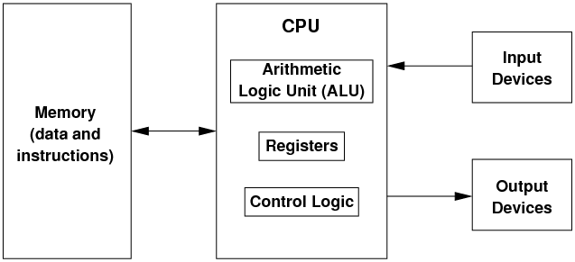
The internal components of a computer normally include CPU, components within a CPU, main memory, buses and I/O controllers. The following block diagram shows how different components of a computer working together as a functional system.
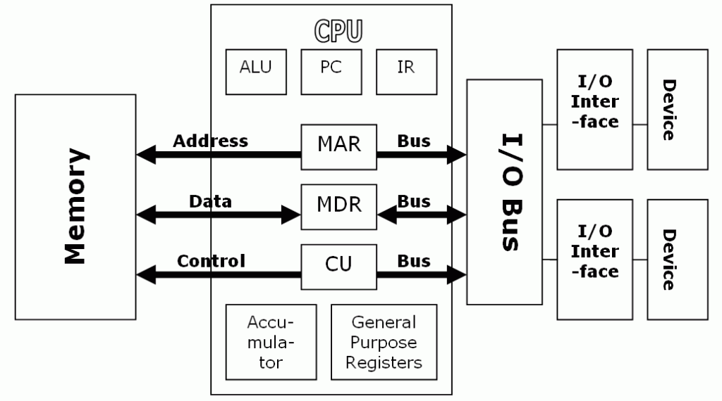
Processor, ALU, Control Unit,Registers, Memory
Objective: understand the role of the following components and how they relate to each other:
ProcessorThe processoris made up by the control unit, the arithemetic logic unit(ALU) and several registers.The control unit- The control unit controls and coordinates all operations.
- It works through a cycle of
fetch,decode, andexecution.- fetch operation fetches the next instruction from the main memeory
- decode operation outputs what the ALU needs to perform on the data
- execution operation causes the instruction to be carried out
The role of control unit can be summarised as below:- To fetch / decode / execute instructions;
- To synchronise operation of processor;
- To marshal/control operation of fetch-execute cycle;
- To send control signals/commands to other components of fetch-execute cycle;
Registers- Registers are small but very fast memory to hold data before and after being processed by the CPU.
- All ALU operations are accomplished within registers.
ALUALU performs addition, subtraction, multiplication, division, comparison(logical ops), and bitwise operations (more later).
Memory- Memory is used to hold temporary instructions and data for manipulation while the system is running.
- When a block of code or data that is held in memory, it is directly accessible to the CPU for manipulation.
- Memory is organised in units called
words. Awordis the maximum number of bits a CPU can process in a single instruction. Typical word size are 8, 16, 32, or 64 bits. - Each word has its own address in the memory.
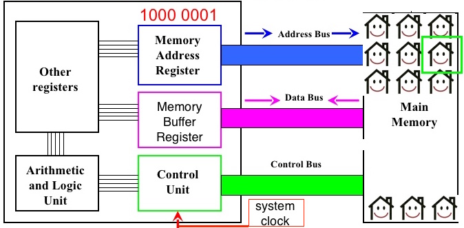
Buses - data bus, control bus and address bus
Objectives: Understand the need for, and means of, communication between components. In particular, understand the concept of a bus and how address, data and control buses are used.
Components communicate with each other using buses. A bus is a set of parallel wires connecting different coomponents. The processor is connected to the main memory by three separate buses. The three types of buses:
Address bus- Address bus is a pathway or a set of parallel wires that carries the location of the data to be read from or written to. An address bus is one directional only - from the processor to the memory or an I/O controller.
- The number of lines for the address bus determines the maximum number of bits it can carry, and in turn determines the maximum possible memory capacity of the computer. To understand this, think if the postal office only allows 3 digits for house numbers, then the maximum addressable houses will be 999. So, if the computer has a 32-bit bus, the maximum addressable memory locations will be 232, which is 4GB, assuming each memory location stores on byte of data.
Data bus- Data bus is a bi-directional pathway or wires that carries data or instructions between computer components.
- The
width of data busis a key factor in determining the overall computer performance. Typical data bus is 8, 16, 32 or 64 bits wide. If a computer has a word size of 32 but with a 16-bit data bus, then the data bus has to fetch the word twice from the main memory.
Control bus- Control bus is a bi-directional pathway that carries command, timing and specific status information among components. The following are some of the control information a control bus may carry:
- write to memory
- read from memory
- write to I/O port
- read from I/O port
- request for data bus
- grant for data bus
- sync clock
- reset all components
- Control bus is a bi-directional pathway that carries command, timing and specific status information among components. The following are some of the control information a control bus may carry:
I/O controllers- An I/O conyroller is a device (an electronic circuit board) that manages the communication between the processor and the I/O device.
- Each I/O device has a separate controller which connects to the control bus.
- I/O controllers receive input and output requests from the pocessor, then send device specific control signals to the device.
- I/O controllers manage the data flow from and to the device.
The von Neumann and Harvard architectures
Objectives: Be able to explain the difference between von Neumann and Harvard architectures and describe where each is typically used.
- von Neumann architecture and the stored program concept
Computer pioneer John von Neumann invented a machine that would hold the instruction and the data to be processed in one single store, the main memory. All computers since then have been built on the same principle.
- In this architecture, the CPU performs the basic computing operations (add, subtract, etc.).
- The CPU gets its data from an external memory, and writes back the results to the memory.
- The memory is also used to hold the program instructions, which control the processing unit and tell it how to manipulate the data.
- The idea of keeping both the data and the instructions in the memory is the essence of the
stored-program architecture. - von Neumann architecture used for general purpose computers.
- Harvard architecture - physical separation of data and instructions
- In this architecture of computers, the data and instructions are stored at two physically different memories. This separation allows some systems to have a read only instruction memory and read-write for data memory. If a system has more instructions than data, then wider address bus can be used for the instruction memory and less wide bus for the data memory.
- Harvard architecture can be faster than von Neumann architecture because data and instructions can be fetched simultaneously.
- Embedded systems such as digital signal processing (DSP) systems use Harvard architecture processors extensively.
- In embedded systems, instructions may be held in read-only memory while data are held in read-write memory.
- Adavantages of Harvard architecture
- Instruction and data can be accessed simultaneously; sAvoid/reduce bottleneck of single data/address buses;
- Instruction and data memory can have different word lengths; Different technologies can be used to implement instruction and data memory;
- Different quantities of instruction and data memory means that address lengths can differ between the two;
- Avoids possibility of data being executed as code, which is one method that can be exploited by hackers;
 Harvard architecture" by Nessa los - Own work. Licensed under CC BY-SA 3.0 via Commons
Understand the concept of addressable memory.
2 The stored program concept
Learn It - describe the stored program concept
The stored program concept has the following properties:
- A machine has the instructions and data being held in the same memory.
- Machine code instructions stored in main memory are fetched, decoded and executed by a processor one at a time.
3 Structure and role of the processor and its components
Learn It - The processor and its components
Objective: Explain the role and operation of a processor and its major components:
- arithmetic logic unit:
A circuit inside a CPU performs the following functions:
- ADD, SUBTRACT, MULTIPLY, DIVIDE
- Arithmetic(signed bit patterns) and logic shift(unsigned bit patterns) on instructions within a register
- Performs logical operations such as AND, XOR, OR, NOT.
- control unit:
- It controls and coordinates the activities within the CPU and control the flow of data in and out of CPU.
- It takes an instruction and decodes it into opcode and operands.
- It manages the execution of the decoded instrcutions, fetches data from location and stores the resultst in memory or registers.
- clock:
- The system clock is used to synchronise CPU operations.
- It generates series of signals of alternating 0 and 1.
- The CPU takes at least one cycle of time (from 0 to 1 or from 1 to 0) to perform one instruction.
- general-purpose registers:
Registersare very fast and small memory inside CPU to hold data before, during and after being processed by the CPU- Typically, a CPU can have up to 16 registers
- Some CPUs only have one general purpose register, called
accumulator.
- dedicated registers, including:
program counter(PC): a special purpose register that holds the address of the next instruction.current instruction register(CIR or IR): holds the currently being executed instruction.memory address register(MAR): holds the memory address to be fetched from or written to.memory buffer register(MBR): a.k.a. memory data register(MDR), holds the data fetched from or written to memory.status register(SR): holds the bits to indicate the results of the execution of an instruction, such as oervflow, negative, zero or carry over.
Learn It - The Fetch-Execute cycle and the role of registers within it
Objective: Explain how the Fetch-Execute cycle is used to execute machine code programs, including the stages in the cycle (fetch, decode, execute) and details of registers used.
When each instruction of a program is being processed by the CPU, it goes through the cycle of three stages:
- fetching: retrieves a program instruction from its memory
- decoding: determines what actions the instruction requires
- executing: carries out the decoded actions
Registers' roles in the fetch-decode-execution cycle can be illustrated in the following flowchart.(You should get familar with the flowchart).
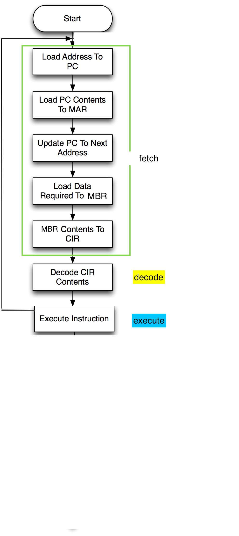
Fetch:
- contents of PC transferred to MAR. MAR<-[PC]
- address bus used to transfer this address to main memory
- contents of addressed memory location moved into the MBR by the data bus, while incrementing PC. MBR<-[Memory]MARaddress; PC<-[PC]+1
- transfer MBR to CIR, ready to be decoded. CIR<-[MBR]
Decode:
- decode instruction held by the CIR by the control unit. decode [CIR]
- instruction split into opcode and operand
Execute:
- if necessary,data is fetched
- the opcode identifies the instruction to execute
- execute instruction by relevant part of processor
- result stored in accumulator
- status register is updated
Click the play button for step-by-step animation of the cycle:
4 The stored program concept
Learn It - describe the stored program concept
The stored program concept has the following properties:
- A machine has the instructions and data being held in the same memory.
- Machine code instructions stored in main memory are fetched, decoded and executed by a processor one at a time.
Learn It - The processor instruction set
Understand the term ‘processor instruction set’ and know that an instruction set is processor specific.
- Processor instruction set means “all the instructions supported by its hardware”
- different processors have different instruction sets
- typical instruction set includes the following common operations:
- LOAD, STORE - data handling and memory operations
- ADD, SUBTRACT, DIVID, MULTIPLY etc - arithmetic operations
- >, <, = etc - comparison operations
- AND, OR, XOR, NOR, NOT etc - logical operations
- Control flow operations - conditional or unconditional
- Logical shifts
- Halt
Know that instructions consist of an opcode and one or more operands (value, memory address or register).
- machine instruction is made of two parts:
opcode: the operation to be performed, and a 2-bit code indicateaddressing modeused for the operationoperands: the value, memory address or register to be operated on
Learn It - Addressing modes
Understand and apply immediate and direct addressing modes.
- machine instruction is made of two parts:
opcode: the operation to be performed- a 2-bit code indicate
addressing modeused for the operation
addressing modesimmediate addressing: the operand is the actual value to be operated on.direct addressing: the operand holds the memory address of the value to be operated on.
Suppose that the opcode 010 means LOAD and the addressing mode 1 indicates direct addressing.
Describe the operation that will be performed by the following machine code instruction:
0101 1100

The above instruction means: LOAD the value from the memory location at 12.
Learn It - Machine-code/assembly language operations
- Understand and apply the basic machine-code operations of:
- load
- add
- subtract
- store
- branching (conditional and unconditional)
- compare
- logical bitwise operators (AND, OR, NOT, XOR)
- logical
- shift right
- shift left
- halt.
Use the basic machine-code operations above when machine-code instructions are expressed in mnemonic form- assembly language, using immediate and direct addressing.
First generation languages: machine code-machine dependant and made of 0s and 1s. Machine code is very difficult to read and debug.Second generation languages: assembly code / assembly language- machine dependant.- Assembly code uses mnemonics to represent the operation codes and addresses.
- Assembler translates assembly code into machine code.
mnemonics examples: LDR, STR, ADD, SUB, MOV, CMP
3rd generation languages: high level programming languages, such as Python, Java, C family etc, which have the following characteristics:- high level of separation from hardware (less dependant on the types of hardware)
- easier for programmers to solve problems and debug
- closer to human language
- Add 12 to the number stored in memory location 52 and save the result in memory location 53.
LDR R0, 52          ; load the contents of location 52 into register 0
ADD R1, R0, #12     ; add 12 to register 0 and store result in register 1
STR R0, 53          ; store the result in memory location 53
- Branching operation 1:
CMP R1, 40 ; Compare value in memory location 40 with value in R1 BGT .next ; if R1 value is greater, go to label .next .next HALT ; label .next which just halts - Branching operation 2:
CMP R1, #100   ; Compare number 100 with value in R1
BNE .loop1    ; if they are not equal, go to label .loop1
- Write assembly code for the following pseudo-code:
pseudo-code:
    X <—- 0
    repeat
     X<—-X + 1
    until X = 99

      CMP R1, #100   ; Compare number 100 with value in R1
      BNE .loop1    ; if they are not equal, go to label .loop1
Assembly Language Operations
The following are some examples of using assembly code. For the list of operations used, please see this page.
Learn It - Factors affecting processor performance
Objective: Explain the effect on processor performance of:
multiple cores:- multiple processors can carry out tasks in parallel.
- A task can also split up to be run on different cores in parallel to speed up execution.
cache memory:- Those are small but very fast memory which located close to CPU. Next instructions or data are stored to be quickly used by the CPU to speed up the execution.
- Depending on how close those cache memories to the CPU, they can be classified as level1,2, 3 etc.
clock speed:- By increasing the clock speed the processor will execute more instructions per unit time.
word length:- The larger the word length, the more data the CPU can process.
- By increasing the word length the processor can access a larger amount of memory through direct addressing.
- By increasing the word length the processor could have a larger instruction set.
address bus width:- By increasing the address bus size we can address more unique memory locations
- Increasing the address bus size increases the maximum potential memory size
data bus width:- By increasing the data bus size we can move more data around per unit time